 Email:
 Telefono:

Miracle PCB
Miracle PWB Technology offers the best PCB services to customers all over the world. We have modern machinery to create or design flawless printed circuit boards. Including multilayer PCB, double-sided PCB boards, 6 layer PCB manufacturing at affordable rates. Our PCB products are used for computer motherboard, communication, digital electronics, automotive, industrial control, aerospace, medical, military, and other electronic assembly industries. Miracle PWB Technology aims to offer high quality printed circuit boards that can be either rigid or flexible based on the customer's requirements. We also offer PCB prototype, PCB fabrication in Shenzhen, China. HDI PCB manufacturing, 6 layer PCB board manufacturing. Get customized PCB services and custom LED PCB board in Shenzhen, China. We promise you will get the quick turn around time, wholesale rates, easy steps to place order and fast shipping. Contact us now or explore our services.
Il time to market rappresenta quanto la puntualità delle consegne dell'azienda sia essenziale per il nostro ..
Il nostro team di esperti CAM Engineering può aiutarti con le modifiche dei dati Gerber secondo le tue esigenze e a un costo minimo.
Una buona comunicazione con i nostri clienti è la chiave per vincere affari.
Miracle Technology creates optimum conditions through its extensive purchasing power, and expertise in PCB industry. We have complete process ownership via a presence both at the customer’s site and in the PCB production factories.

QUALI SERVIZI FORNIAMO
i nostri servizi principali hanno due direzioni e sono garantiti
We provide full PCB production services in Shenzhen, China, which are fully customizable, not only with high reliability but also guaranteed to fully meet your requirements. PCB production business covers rigid FR4, PCB, HDI PCB, 6 layer PCB manufacturing, 2 layer PCB manufacturing FPC, aluminium PCB, Rogers PCB, etc.
- 11 Capacità di produzione ampliate
- 12 Rigorose opzioni di controllo della qualità
- 13 Opzioni a valore aggiunto: DFM GRATUITO e altro ancora
- 14 Preventivo online e sistema di ordini
Forniamo servizi completi di produzione di PCB a Shenzhen, in Cina, che sono completamente personalizzabili, non solo con elevata affidabilità ma anche garantiti per soddisfare pienamente le vostre esigenze. L'attività di produzione di PCB copre FR4 rigidi, PCB, PCB HDI, FPC, PCB in alluminio, Rogers PCB, ecc.
- 21 Capacità di produzione ampliate
- 22 Rigorose opzioni di controllo della qualità
- 23 Opzioni a valore aggiunto: DFM GRATUITO e altro ancora
- 24 Preventivo in linea e sistema di ordini
PERCHÉ SCEGLIERCI
i nostri punti di forza sono abbastanza convincenti e molto di più
Servizio di selezione dei materiali, valutazione DFM, ruoli di progettazione, soluzione economica, ecc.
Una logistica completa e perfetta supporta operazioni personalizzate e professionali, fornendo ai nostri clienti servizi ed esperienza di consegna flessibili, efficienti e di alta qualità.
Abbiamo un perfetto servizio post-vendita e la successiva garanzia della qualità del prodotto è uno dei nostri servizi.
Serve mercati che coprono più di 150 paesi nei quattro oceani
Il numero totale dei dipendenti ha superato le 500 persone
Durante dieci anni di attività, il nostro tasso di consegna puntuale è superiore al 98,5%
Oltre 1000 clienti in collaborazione, il tasso di visita di ritorno del cliente è del 40%
PCB manufacturing and PCB Assembly Services
PCB manufacturing:
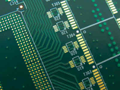
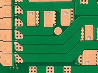
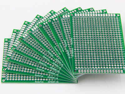
It’s a printed circuit board (PCB). Insulating and conductive layers are sandwiched between one other on the printed circuit board (PCB).
PCB supports electronic circuit parts mechanically. The PCB components that have been soldered together are electrically and mechanically more efficient. Conventional printed circuit boards (PCBs) are used in all electrical products to link various components of the circuit.
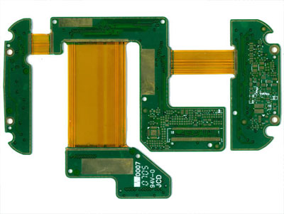
Multilayer PCB Manufacturing or Fabrication:
We also do 6 layer PCB fabrication. It is possible to manufacture 6 layer PCBs using either single-sided (with a single copper layer) or double-sided (with two copper layers on either side of a single substrate layer) PCBs.
Because circuit traces on the inner layers would otherwise occupy surface space between components, multi-layer PCBs take into account a much higher part thickness. When surface mount technology became widely accepted, multi-layer PCBs with more than two, and especially four, copper planes became increasingly common. So, contact us for flawless multilayer or 6 layer PCB manufacturing.
PCB DESIGN From Miracle PWB:
The design of a PCB has a lot to do with how well it works. It is a very important thing to do if you want your board to work better.
Modern PCBs are made with the help of software. First, this software is used to make a schematic diagram of a circuit. Then, that schematic diagram is turned into a PCB layout. PCB CAM is used to do the following,
- Input of the fabrication data.
- Verification of the data
- Compensation for deviations in the manufacturing processes
- Output of the digital tools
The size of the PCB board is chosen based on the design of the PCB and the design of the machine where it will go. The design of the product also determines where the different parts go.
The Process Of PCB manufacturing
It is the process of converting a circuit board’s design into a physical structure by following the design parameters specified. The following acts or procedures are used to generate this physical design:
- A copper-clad laminated image of the intended design arrangement
- Revealing tracks and pads by etching or removing copper from the inner layers
- Laminating (heating and pressing) board materials at high temperatures to create the PCB layer stackup
- Boring holes for mounting holes and vias, as well as drilling holes for through-hole pins
- exposing the traces and pads by etching or removing superfluous copper from the top or topmost layer(s).
- Plated pin and via holes.
- Surface or solder masking protection by applying a protective layer
- Indicators of polarity and other identifiers, such as logos, can be silkscreen printed on the surface.
- Copper surfaces can have a finish applied as an extra option.
- The Etching: Etching requires extreme caution so that the solution does not irritate or otherwise injure the skin.
What Do We Offer?
There are a variety of PCB technologies and fabrication techniques that Miracle PWB can provide:
PCB development:
To put it another way, PCB development is the process of taking an idea for a circuit board from the drawing board to the assembly line. Most of the time, this process has three steps: design, production, and verification or validation. This is an iterative method that tries to come up with the best design possible in the time given, except for the simplest ideas.
PCB Manufacturing or PCB Fabrication:
Creating a printed circuit board (PCB) is the process of building a prototype of your idea. Board fabrication and printed circuit board assembly are two separate processes (PCBA).
PCB testing:
The third stage of PCB development, PCB testing, after production. Testing is done during development to make sure the board can do its intended functions. Therefore, in this phase, mistakes and design improvements are found. A new cycle starts to include the design improvement.
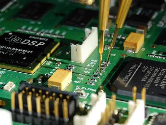
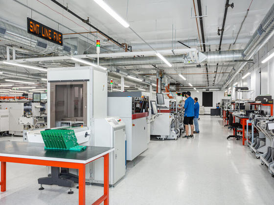
PCB Assembly, PCBA:
PCB Assembly, often known as PCBA, is the second stage of PCB manufacturing. It involves connecting the board components to the bare board.
What are the basic parts of a PCB?
When we talk about PCB manufacturing, a printed circuit board is composed of four fundamental components:
The substrate, which is typically constructed of fiberglass, is the initial step in the process. Fiberglass is utilized on PCBs because it adds structural integrity and prevents the boards from shattering. Substrates are like the “skeleton” of a PCB.
Copper Layer: This layer can be either copper foil or a full-on copper coating depending on the board type. Whichever method is employed to make use of the copper, its primary purpose remains the same: conveying the electrical signals between the PCB and other components.
The solder mask serves as the PCB’s “skin” in this manner. In order to prevent copper from short-circuiting when it comes into touch with the environment, the PCB’s solder mask is included as the final component.
Silkscreen: Finally, the circuit board is completed with a silkscreen. Part numbers, logos, switch settings, component reference, and test points are typically shown on the component side of the board using silkscreen.
“Even the simplest digital electronics, like digital clocks, calculators, and so on, have these amazing inventions. In simple terms, a printed circuit board (PCB) is a board that moves electrical impulses from one place to another. In a nutshell, PCBs control the flow of electricity, which is what makes your electronics work”.
About MIRACLE PCB:
Miracle Technology is a Chinese corporation with headquarters in Shenzhen that exports electronic goods and components of high quality to markets all over the world.
Miracle Technology plans to offer PCB manufacturing services to all of its customers. Morover these services will include master configuration, production, a production network, request fulfillment, and exchange arrangements for resellers. We provide printed circuit board (PCB) sheets for use in a diverse array of applications, including those in the computer, communication, consumer electronics, automotive, industrial control, aerospace, medical, military, and other electronic assembly industries.
Depending on the requirements of your project, you can choose from a variety of different types of printed circuit boards (PCBs), such as single-sided boards, double sided pcb boards, multilayer boards, 6 layer PCB manufacturing, PCB Fabrication, HDI boards, flexible boards, rigid-flexible boards, special process boards, and material boards.
Our Capacity:
Miracle PCBs are currently serving customers in over 150 countries across a vast array of markets. There are more than 500 workers on staff, and the percentage of on-time deliveries achieved throughout the company’s first business is 98.5 percent.
Because of our capabilities, Miracle PWB’s ability is to deliver PCB manufacturing services on time. Our goal is to help our clients get the best chance to get ahead by making printed circuit boards (PCBs) at the lowest possible total cost.
Why Should You Pick the Miracle PCB?
- A PCB prototype manufacturer that is both reputable and professional
- Quick turn around services for PCB assembly
- The minimum number of pieces per order for PCB is one.
- The prototype with the quickest PCB
- Customer service available online around the clock
- PCB engineer with professional experience for one-to-one service
- Quality that is guaranteed from the time of the PCB quote till delivery
- Reduced the amount of time it takes for DHL deliveries to merely 3-5 days
- Efficient in terms of costs
- Advanced prototype PCB assembly capabilities
