 Email:
 Phone:

What Is A PCB? The Ultimate Guide On A PCB Assembly
2022-09-06What is a printed circuit board, or What is a PCB? PCB Explained.
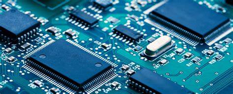
You may be trying to find the best answer to the question “What is a pcb?” A printed circuit board, or PCB, is made of an electrically insulating material (like getinax, textolite, fibreglass, or other similar dielectrics). That has thin conductive plates (called “printed conductors”) on its surface. It has pads that can be used to connect and install radio parts like modules and integrated circuits.
These are electronic components used widely now a days.
So that’s another answer to the question, “What is a PCB?” A printed circuit board is a piece of equipment that has fixed electrical connections on a base that doesn’t conduct electricity. There are also multi layered pcbs that are used in special purposes.
A printed circuit board has a rigid or flexible dielectric base and conductors on its surface. PCBs have dielectrics and conductors. These are the only two parts that make it a printed circuit board.
Contact pads, metallized transitions and mounting holes, connector lamellas, heat-removing sections, shielding and current-carrying surfaces, etc are used to put the parts in place and connect them to the wires.
It was a huge step forward when electronic equipment design switched to PCBs. A PCB holds and connects radio parts. If there isn’t enough insulation resistance between PCB conductors and other conductive parts, the second function can’t happen. The PCB’s base must therefore be insulating.
The history of printed circuit boards is told in the following way:
To learn more about what is a pcb? Let’s begin. At the start of the 20th century, a German engineer named Albert Parker Hanson worked on making phones work. He made something that is thought to be the first type of printed circuit board ever made.
People think that printed circuit boards “came into being” in the year 1902. When the inventor put in a request for a patent with the office in his home country.
Hansen’s circuit board was made from bronze (or copper) foil that was stamped or cut out. The conductive layer that was made was then stuck to a dielectric, which was paraffin-soaked paper. Even so, Hansen pasted the foil on both sides to make sure there were more conductors. This made a double-sided printed circuit board.
The person who made the printed circuit board also used holes to connect things. Hansen’s works explain how conductors are made using electroplating or conductive inks, which are made of metal powder mixed with an adhesive.

History Explained: What is a PCB?
At first, only “additive” technologies were used to make printed circuit boards. This means that the pattern was put on the dielectric by gluing or spraying material.
Thomas Edison had some of the same ideas. Edison wrote a letter to Frank Sprague, who later started Sprague Electric, in which he explained three ways to draw a conductor.
1. The pattern is made by sticking graphite or bronze to a surface that is free of dust and then crushing them into dust.
2. The pattern is made on the dielectric itself. Lapis (silver nitrate) is used to make the image, and then salt is used to get the silver back.
The conductor is a piece of gold foil with a design on it.
Scientists Explained, what is a PCB?
Even though Edison didn’t use the term “printed circuit boards,” almost all of the ideas above are still used in technology today. Today’s thin-film technologies are based on the first of these. By removing metals from salt, the second method is often used to coat things.
Arthur Berry got a patent for his way of making printed circuit boards by taking away parts. The developer suggested covering the metal base with a layer of resistive material and etching away parts of the surface that are not protected. Ellis Bassit from the United States came up with and got a patent for a way to use photosensitive materials to make printed circuit boards in 1922.
Charles Duclas, an American, came up with the idea of metallization of conductors. The basic idea was to fill channels with a soft dielectric (for example, wax). Which were then filled with conductive pastes made of metal by an electrochemical process.
More details about What is a PCB?:
Many patents were given out in the 1920s and 1930s for the design of printed circuit boards and the ways to make them. Most of the first methods used to make printed circuit boards were still additive (the development of the ideas of Thomas Edison). But the printed circuit board as we know it today came about because printing technology was used to make it.
The English word “printing plate,” which means “printed form” or “matrix,” is the exact same thing as “printed circuit board.” So, the real “father of printed circuit boards” is thought to be the Austrian engineer Paul Eisler.
He was the first person to figure out that printing (subtractive) technologies can be used to make printed circuit boards in large quantities. In subtractive technologies, an image is made by taking away bits that aren’t needed. Paul Eisler figured out how to galvanically deposit copper foil and use chlorine iron to etch it.
How Is PCB Assembly Done?
So, when we ask, “What is a PCB board?” it’s important to understand the materials involved in PCB assembly services. Table 1 summarizes MPP’s key types, sizes, and features. Most Printed Circuit Boards are built with conventional fibreglass laminate type better known as FR4, which may be used from –50 to +110°C and has a glass transition temperature (Tg) of about 135°C.
Dk ranges from 3.8 to 4.5 depending on supplier and material. High-temperature FR4 High Tg or FR5 is used to strengthen heat resistance or for lead-free oven mounting (up to 260 °C).
Polyimide is utilized for high-temperature operations or abrupt temperature shifts. Polyimide is also utilized to produce more reliable military and civilian circuit boards.
These materials cost more than FR4, as seen in table 1’s last column. Figures 4, 5, and 6 illustrate dielectric boards. Everyone who uses single-layer or multi-layer PCBs must know their materials.
Single-layer PCBs are used in high-speed and microwave devices. Developers must compute wave impedance of board conductors, high-voltage insulation between layers, and blind/hidden hole structure.
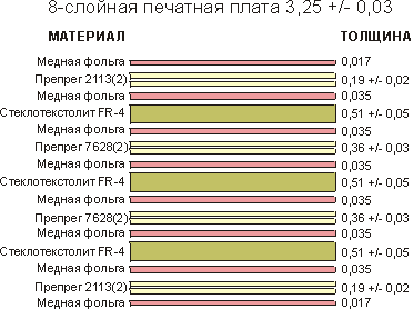
Tables 2–6 indicate alternatives and thicknesses. Material thickness can be off by up to 10%, so the finished multilayer board can’t be off by less than 10%.
To order the best PCB assembly services, prototype pcb assembly from an expert company contact us now. Click here
What are the Materials used for printed circuit boards and how they are used?
Typical PCB designs for the best Printed Circuit Board are based on using standard FR4 fibreglass, which has an operating temperature range of –50 to +110 ° C and a glass transition temperature Tg (softening) of about 135 ° C.
What is a PCB in high-temperature? FR4 High Tg or FR5 is used when heat resistance needs to be better or when mounting boards in an oven using lead-free technology (up to 260 °C).
Polyimide is used when there is a need for continuous work at high temperatures or sudden changes in temperature. Polyimide is also used to make more reliable circuit boards, both for the military and in other situations where electrical strength needs to be increased.
Dielectric constant
Why and how do PCBs work? Consider the soldering pads’ copper coverings. Covering the locations usually involves tin-lead alloy, or PIC. The process of putting solder on a surface and making it even is called HAL or HASL.
These terms come from the English phrase “Hot Air Solder Leveling,” which means “levelling the solder with hot air.” This coating makes soldering easy. Nowadays the modern, RoHS-compliant coatings are replacing it meeting the international level.
This directive specifies products can’t include lead. RoHS doesn’t applicable to our country yet, but it’s worth remembering.
“Table 7 illustrates MPP coverage options.”.
Immersion gilding evens up the board’s surface, which is necessary for BGA pads. It makes soldering harder. Soldering by hand requires particular fluxes, although furnace soldering is equivalent to HASL. Organic coatings prevent copper from oxidizing.
Note: Solderability is short-lived (less than 6 months).
Immersion tin works well for soldering but has a short shelf life. Lead-free HAL has the same qualities as lead-containing HAL, but it’s 99.8% tin and 0.2% other components.
When the board is in use, the contacts of the knife connectors that move against each other are coated with a thicker and more rigid layer of golden finger. For both kinds of gilding, a nickel layer is used to stop gold from spreading.
Insulating coatings are used to cover the sides of conductors that aren’t meant to be soldered.
What is a PCB in marking?
Paint is put on the board over the mask to make it easier to figure out what the board is and what parts are on it.
Peel-off mask: This is put on parts of the board that need to be protected temporarily, like from soldering. In the future, it will be easy to take off because it is made of a rubber-like material that just peels off.
Carbon contact coating is put on parts of the board where keyboards make contact. The coating is good at conducting electricity, doesn’t rust, and doesn’t wear away easily.
Resistive elements made of graphite can be put on the surface of the board to act as resistors. Unfortunately, the values are not very accurate. They are not more accurate than 20% (with laser adjustment, they can be up to 5%).
Silver contact jumpers can be used as extra conductors to add another layer of conductivity where there isn’t enough room for tracing. They are mostly used to make printed circuit boards with one layer or two.
What are PCBs? What is PCB Fabricator?
A simple wire, which is usually wrapped in insulation, is the most basic thing that came before printed circuit boards.
We employed radio element carriers, radio elements, and structural elements to link and fix the cables. It’s a space-themed installation.
PCBs lack these problems. Their conductors are anchored to the surface, so they can figure out how to link. PCB designs are becoming flatter.
One-sided PCB: or One-sided PCB: Flat metal with printed wires. Conductors utilised the empty back side of double-sided PCBs.
Fig. 1 shows single- and double-sided PCBs.
What is a printed circuit board with only one side? or What is a PCB with only one side? It is a flat piece of metal with printed wires on one side. In double-sided printed circuit boards, the empty back side of the plate was also used by the conductors.
In Fig. 1, you can see small pieces of the simplest single-sided and double-sided printed circuit boards.
What is a PCB board with two sides?
Types of PCB are explained along with the manufacturing process.
The first step from the plane to the volume was to use them instead of single-sided paper. Without a double-sided PCB’s substrate, conductors form a three-dimensional structure. This step was fast. Albert Hanson’s application mentions putting conductors on both sides of the substrate and connecting them via holes.
Microelectronics, the newest innovation in electronics, has led to the use of components with more than one pin (a chip can have over 200 pins). Digital microcircuits and their increased speed have made it increasingly vital to protect them and ensure electricity reaches all of their parts. Digital multilayer boards feature shielding conductive layers. (Computers)
More connections and more sophisticated connections led to more layers. Modern PCBs have more than ten. Multilayer PCBs have grown.
How to design printed circuit boards with more than one layer?
Consider a multilayer board. In the most prevalent version, the board’s inner layers are copper-laminated fibreglass. The “core” Outside layers are copper foil glued to internal layers with “prepreg.”
High-temperature pressing creates a “pie”-shaped multilayer PCB. Pie is drilled and metallized. Second option is less typical when outer layers are prepregged “cores.”
There are various design options based on these considerations. Prepreg holds layers together. Two bilateral “cores” can’t touch without a prepreg gasket, but a foil-prepreg-foil-prepreg-foil-prepreg-foil-prepreg-foil-prepreg-foil-prepreg-foil-prepreg-foil-prepreg-foil-prepreg- It’s utilized on boards with many hidden holes.
Two-thirds of all PCBs created worldwide are now multilayer boards. Smaller than single- and double-sided boards.
Fig. 2 depicts a simplified schematic of a multilayer PCB. Conductors are within and on the surface of these PCBs. The conductors’ layers were also preserved in the same spot (a consequence of the use of planar printing technologies).
Looking for double sided, 6 layer PCb manufacturing, 8 layer PCB manufacturing with high quality and highly reliable service? Visit miraclePWB now.
One-sided, double-sided, and multilayer PCB boards.
The names of printed circuit boards and their parts always have something to do with layering, like “one-sided,” “double-sided,” “multi-layer,” etc.
Interlayer transitions (vias) and micro-transitions (microvias) are used to switch between the layers of MPP. Fig. 3.a. Interlayer transitions can be done as through holes that connect the outer layers to each other and to the inner layers.
There are also blind and hidden changes for Rigid PCBs
- Blind transitions are metal-lined channels that link board pieces. It’s only visible from above or below.
- Hidden transitions connect inner board layers. Wiring boards is easy with them. 12-layer MPP can work like 8-ply commutation, for example.
- Surface-mounted micro junctions connect contact and signal layers.
- Laminated dielectric foil is glued together with “prepregs” to make multilayer PCBs.
- Figure 3 shows prepreg in white. Prepreg glues PCB layers when heated and pressed.
- When the number of signal layers on a PCB or multilayer PCB increases, so does its thickness.
- In this scenario, board thickness vs hole size is a hard parameter for through-hole metallization.
- Multilayer PCB makers seek to build boards with a high installation density by using a large number of cheap layers instead of a small number of high-density, more expensive layers.
- Figure 3.c displays the layers and thickness of a multilayer PCB.
